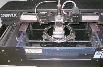
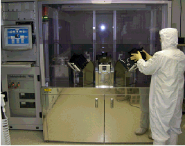
The latest bonding and inspection
equipment is used to manufacture
SOI and GeOI bonded wafers
equipment is used to manufacture
SOI and GeOI bonded wafers
| | | |
| Semiconductor Processing Company 12 Channel Street #702 Boston, MA 02210 Voice (617) 345-9936 FAX (617) 345-9271 |
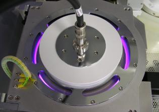
Plasma activation lowers anneal temperatures,
enhances bond strength and also allows for
bonding of thermally mismatched materials.
enhances bond strength and also allows for
bonding of thermally mismatched materials.
CSAM
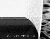
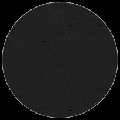
| Void Free |
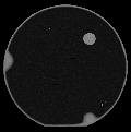
| Void Detection |
Wafer Surface Characterization Standard Bonding or Plasma Bonding High Temp or Low Temp Annealing 100% Acoustic Interface Imaging |